 IC Development
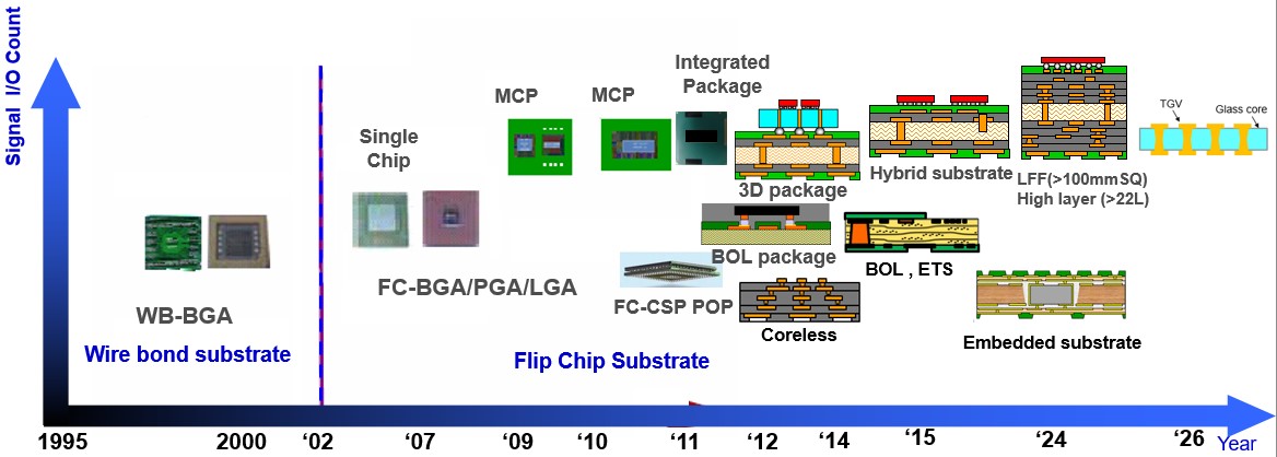

In response to greater trace density, transmission efficiency and against to signal disturbing, the way of packaging has been transformed into flip chip from wire bonding.
To make electronic production slim and with multi-functions, single- chip package is supposed to be replaced by MCP (Multi-chip package) in the future.
Wire bonding is gradually replaced by flip chip and the layout would move to thin core, fine line and fine pitch design.
According to the increasing chip processing speed and high I / O requirements, the flip-chip substrate faces fine bump pitch from packaging. In order to achieve UBM copper pillar package,the substrate will have an another way for BOT (bump on trace) design. In addition, 3D package technology will be next generation and fine bump density , high rigid substrate are needed for this technology as well.
We will continue to develop high layer count(>22L), LFF(>100mmSQ) and embedded substrate to meet customer's 5G 、AI & HPC (High Performance Computing) application.